Purpose
RT4832A is an integrated total power solution for Flash
LED Driver, Backlight WLED Driver, and DSV Driver. This document explains the
function and use of the RT4832A evaluation board (EVB), and provides information
to enable operation, modification of the evaluation board and circuit to suit
individual requirements.
Introduction
General Product Information
RT4832A is an integrated total power solution for Flash LED
Driver, Backlight WLED Driver, and DSV Driver. Flash LED Driver provides up
to 2-CH 1.5A applications. Back Light WLED Driver supports up to 36V output
for 10 WLEDs applications. And it provides 1024 steps LED current with logarithmic/linear
curve. DSV is implemented by one single inductor boost and inverting charge
pump, which provide customers minimum EVB Area compared to dual inductors. The
negative output power (CPOUT) comes from boost output (LCMOUT). It also provides
DSV positive voltage (POS), which power noise is reduce by passing though LDO.
Their ranges can be programmed from ±4V to ±6V per 50mV step respectively. Flash
Boost Converter operates at 2MHz/4MHz frequency. The 4MHz frequency solution
allows tinny and low-profile components. Torch Mode Current can be set from
25mA to 375mA per 25mA Step. And Strobe Mode Current range is from 100mA to
1.5A per 100mA Step.
DSV drives TFT-LCD panels up to 10” (from SFF to MFF like tablets).
These two output rails are usually connected to Source Driver IC. Wide input
voltage range from 2.5V to 5.5V optimizes the single-cell battery applications
(Li-Ion, Ni-Li, Li-Polymer) and which symmetrical output current is up to 80mA.
The RT4832A provides complete protection such as VIN under voltage
lockout, Vin monitor protection, over current protection, over voltage protection,
LED short protection, VOUT short protection and over temperature protection.
RT4832A is available in WL-CSP-30B 2.24x2.64 (BSC) package.
Product Feature
- Input Voltage Range: 2.5V to 5.5V
- Internal Soft-start, UVLO, OTP, OCP
- Typical Shutdown Current: < 1μA
- -40 to +85°C Temperature Range
- 2CH Back Light LED Driver
♦ Drives up to 10 WLEDs in Two Strings
♦ External PWM Pin Control and I2C Programmable 11
bit Linear and Exponential Brightness
♦ LED Current Accuracy ±5%
(>500μA), ±3% (>5mA)
♦ I2C Programmable OVP 18/22/25/29/33/36V
- 2CH Flash LED Driver
♦ Torch Mode Current from 25mA to 375mA
per 25mA Step with 2 channels
♦ Strobe Mode Current from 100mA
to 1.5A per 100mA Step with 2 channels
♦ I2C Programmable
Flash Safety Timer from 32msec to 1024msec per 32msec Step
- High Accurate Safety Timer ±10%, Current Accuracy ±4% (>375mA), Current
Matching ±7%(>375mA)
♦ VIN Monitor Protection from 2.5V to
3.2V per 0.1V Step
♦ Selectable Input Current Limit 1.9A /2.8A
♦ 2MHz/4MHz Switching Frequency for Flash LED
♦ Flash
LED1/2 Short Protection, and Output Short Protection
♦ Txmask
Protection by Independent Pin
- DSV
♦ I2C Programmable Output Voltages
♦
Flexible Boost Voltage, POS, CPOUT Default Setting
♦ Regulated
Voltage Output: 4V to 6V per 50mV Step
♦ Positive Voltage Output:
4V to 6V per 50mV Step
♦ Negative Voltage Output: -4V to -6V per
50mV Step
♦ User Selectable Output Fast Discharge Mode or Float
Mode when turned off
♦ Independent Positive and Negative Enable
Control by Two External Pins
♦ True Load Disconnect, OCP, and
Positive/Negative SCP Function
Key Performance Summary Table
|
Key Features
|
Evaluation Board Number: PCB092_V1
|
|
Input Voltage Range
|
2.5V ~ 5.5V
|
|
Flash LED Strobe Current*
|
25mA ~ 375mA
|
|
Flash LED Torch Current*
|
0.1A ~ 1.5A
|
|
LED OVP Voltage*
|
18V ~ 36V
|
|
LED Output Current*
|
0 ~ 25mA
|
|
POS Voltage*
|
4V ~ 6V
|
|
CPOUT Voltage*
|
-6V ~ -4V
|
Bench Test Setup Conditions
Headers Description and Placement
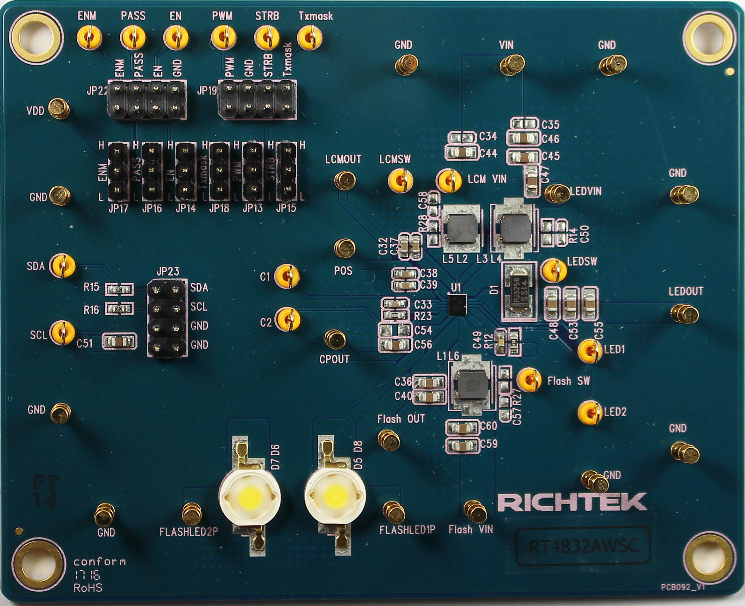
Carefully inspect all the components used in the EVB according
to the following Bill of Materials table, and then make sure all the components
are undamaged and correctly installed. If there is any missing or damaged component,
which may occur during transportation, please contact our distributors or e-mail
us at evb_service@richtek.com.
Test Points
The EVB is provided with the test points and pin names
listed in the table below.
|
Test point/
Pin name
|
Signal
|
Comment (expected waveforms or voltage levels
on test points)
|
|
VIN
|
Input voltage
|
Power input. Support 2.5V to 5.5V Input Voltage.
Must bypass with a suitable large ceramic capacitor at this pin.
|
|
LCMOUT
|
Enable test point
|
DSV boost converter output pin.
|
|
POS
|
Output point
|
DSV positive output pin.
|
|
CPOUT
|
Output point
|
DSV negative output pin.
|
|
LCMSW
|
Switch node test point
|
Switching node of DSV boost converter. Connect
a 2.2μH inductor between LCMSW and VIN.
|
|
LEDSW
|
Switch node test point
|
Switch node of boost converter. Connect a 4.7μH
to 10μH inductor between LEDSW and VIN.
|
|
LEDOUT
|
Output point
|
Backlight boost converter output pin.
|
|
LED1
|
Input point
|
Backlight current sink 1.
|
|
LED2
|
Input point
|
Backlight current sink 2.
|
|
Flash SW
|
Switch node test point
|
Drain connection for internal N-MOSFET and synchronous
P-MOSFET switches. Connect a 0.47μH to 1μH inductor between FlashSW
and VIN.
|
|
Flash OUT
|
Output point
|
Flash boost converter output pin.
|
|
FLASHILED1S
|
Output point
|
Flash current source 1.
|
|
FLASHILED2S
|
Output point
|
Flash current source 2.
|
|
GND
|
Ground
|
Ground.
|
Power-up & Measurement Procedure
1. Connect input power (2.5V < VIN <
5.5V) and connect the EN pin to H level for the chip enable.
2. The slave address is 7b’0x11. Check the register
table and modify it if need.
3. Write 0x0C = 0x48 to enable the DSV. Write 0x0A
= 0x19 to enable backlight. Write 0x0A = 0x02 to enable flash LED.
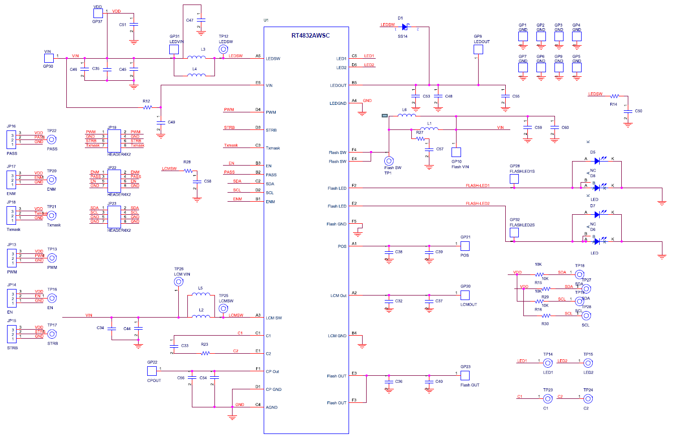
Schematic, Bill of Materials & Board Layout
EVB Schematic Diagram
Bill of Materials
|
Reference
|
Qty
|
Part number
|
Description
|
Package
|
Manufacture
|
|
U1
|
1
|
RT4832AWSC
|
Boost Converter
|
WL-CSP-30B 2.24x2.64
|
RICHTEK
|
|
C32, C37, C38, C39
|
4
|
GRM188R61C475KAAJD
|
4.7µF/16V/X5R/0603
|
C-0603
|
MuRata
|
|
C33
|
1
|
C1608X5R1E105KT000E
|
1µF/25V/X5R/0603
|
C-0603
|
TDK
|
|
C36, C40, C48, C53, C55, C59, C60
|
7
|
CGA4J3X5R1H475K125AB
|
4.7µF/50V/X5R/0805
|
C-0805
|
TDK
|
|
C44, C45, C46, C47, C51, C56
|
6
|
C2012X5R1C106KT
|
10µF/16V/X5R/0805
|
C-0805
|
TDK
|
|
C49
|
1
|
0603B103K500
|
10nF/16V/X7R/0603
|
C-0603
|
WALSIN
|
|
D1
|
1
|
SS14
|
SS14
|
D-D
|
PANJIT
|
|
D6, D8
|
2
|
P2000L‐W2O1‐A1J11H
|
Flash LED
|
P2O_LED_2
|
SemiLED
|
|
L3
|
1
|
NR4018T100M
|
10µH
|
4.0*4.0
|
TAIYO YUDEN
|
|
L5
|
1
|
NR4018T2R2M
|
2.2µH
|
4.0*4.0
|
TAIYO YUDEN
|
|
L6
|
1
|
NR4018T1R0N
|
1µH
|
4.0*4.0
|
TAIYO YUDEN
|
|
R12
|
1
|
WR06X1500FTL
|
150/0603/ ±1%
|
R-0603
|
WALSIN
|
|
R15, R16
|
2
|
WR06X1002FTL
|
10K/0603/ ±1%
|
R-0603
|
WALSIN
|
|
R23
|
1
|
WR06X000 PTL
|
0/0603 / ±1%
|
R-0603
|
WALSIN
|
PCB Layout
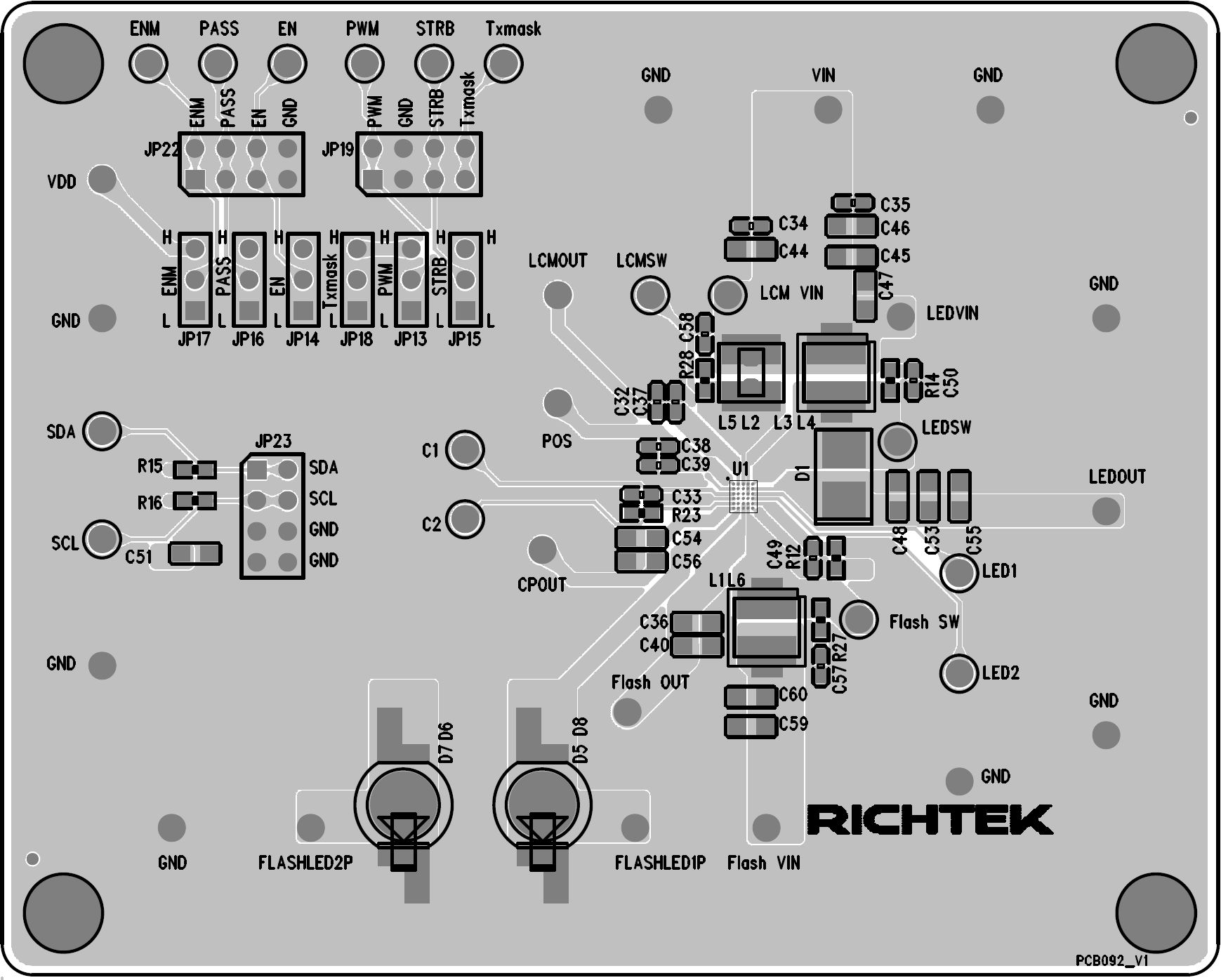
Top View (1st layer)

PCB Layout—Inner Side (2nd Layer)
PCB Layout—Inner Side (3rd Layer)
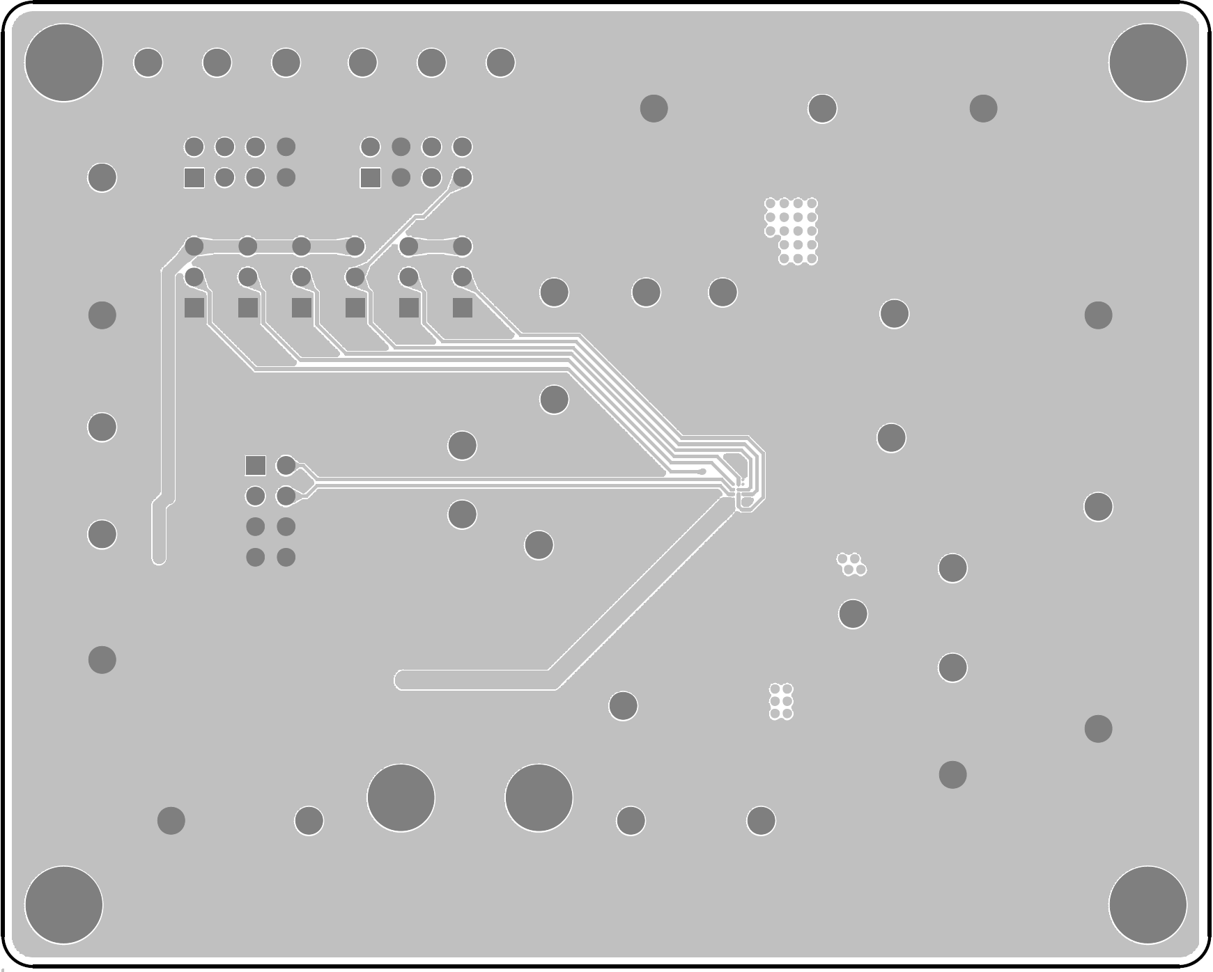
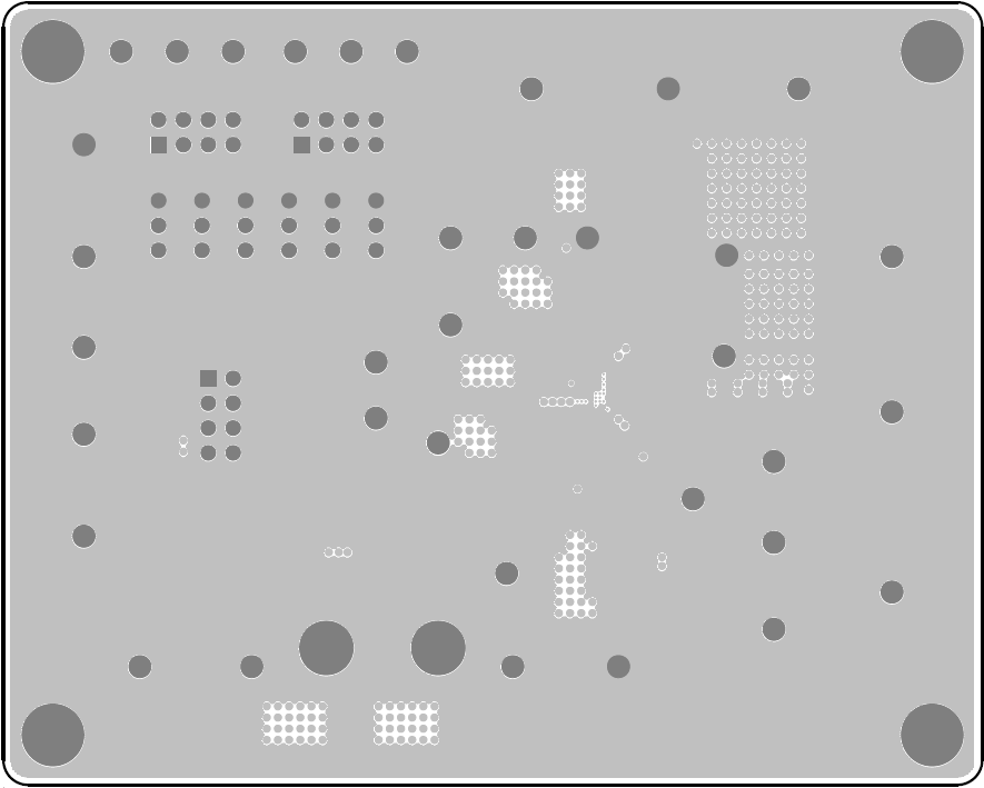
Bottom View (4th Layer)